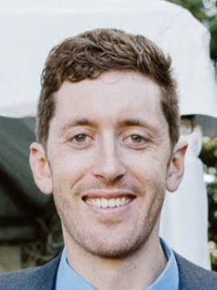
Tom Pekin, PhD

After 9 years in academia, I recently (Jan. 2023) switched to my current position as a Team Product Owner at the semiconductor mask solutions (SMS) branch of Carl Zeiss SMT, located in Jena, Germany. More info will come as I learn what I can talk about and not 🙃.
Prior to the switch to industry, I was a a postdoc at the Humboldt Universität zu Berlin, where I was a member of Christoph Koch’s Structure Research and Electron Microscopy group. There I worked on developing ptychographic methods using electron microscopy and high-end STEM/EELS on a Nion UltraSTEM. Previously, I did my PhD under Andrew Minor at UC Berkeley and the National Center for Electron Microscopy, where I focused on method development at the intersection of electron microscopy and structural materials science.
My research interests included electron ptychography and computational microscopy, as well as combining in situ electron microscopy methods with 4DSTEM techniques, with the hope of discovering new structure-property relationships that could then be exploited to improve material properties. I enjoyed working with diverse classes of materials, including catalytic materials, bulk metallic glasses, structural steels, and 2D materials like MoS2 and graphene. I also enjoyed teaching and incorporating Python into physics and materials science courses and research.
Outside of work I enjoy live music, various water sports, coding, and learning German.